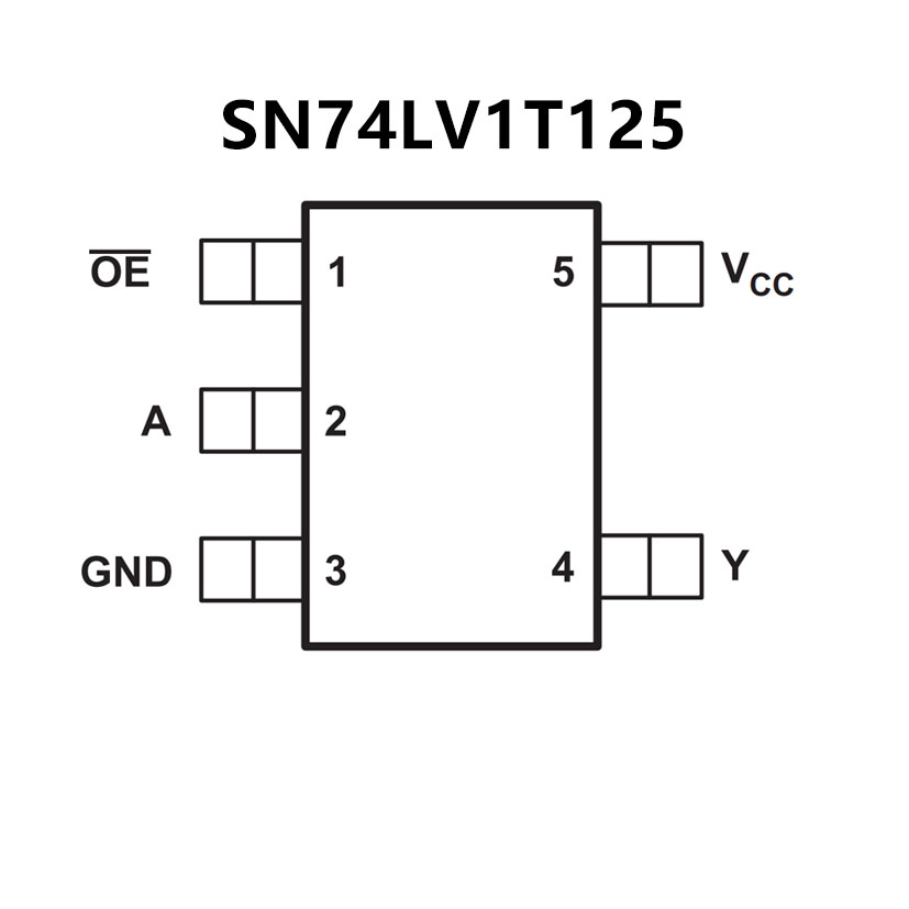


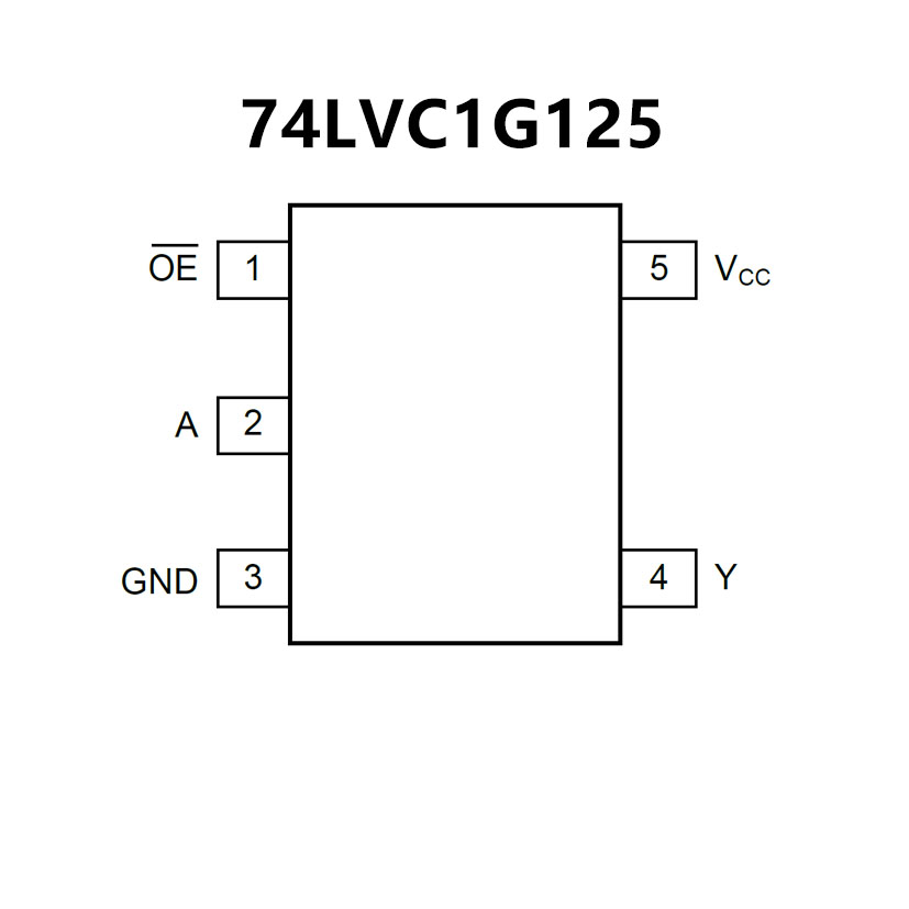
 74LVC1G125.pdf
? Wide Supply Voltage Range: 1.65V to 5.5V
? High Noise Immunity
? ±24mA Output Drive at VCC = 3.0V
? CMOS Low Power Consumption
? Inputs Accept Voltages Up to 5V
? Direct Interface with TTL Levels
? -40℃ to +125℃ Operating Temperature Range
? Available in a Green SC70-5 Package
? Single-Supply Voltage Trans1ator at
5.0/3.3/2.5/1.8v vcc
? Operating Range of 1.8v to 5.5vUp Trans1ation
1.2V(1) to 1.8V at 1.8v Vcc
1.5V(1) to 2.5V at 2.5v vcc
1.8V(1) to 3.3V at 3.3v vcc
3.3V to 5.0v at 5.ovvcc.
? Down Trans1ation
3.3v to 1.8v at 1.8v vcc
3.3 V to 2.5v at 2.5v vcc
5.0v to 3.3v at 3.3v vcc.
? Logic Output is Referenced to vcc. output Drive
8.0mA Output Drive at 5.ov
7.0mA Output Drive at 3.3 v
3.0mA Output Drive at 1.8v
? Characterized up to 50MHz at 3.3v vcc
? 5.0V Tolerance on Input Pins
? -40°C to 125C Operating Temperature Range
? Latch-Up Performance Exceeds 250mA
Per JESD 17
? ESD Performance Tested Per JESD 22
200o-V Human-Body Mode1
(A114-B,C1ass II)
200-V Machine Mode1 (A115-A)
1000-v Charged-Device Mode1 (C101)
? Supports Standard Logic Pinouts
? CMos Output B Compatib1e with AUP1G and
LVC1G Families
(1)Refer to the VIH/VILand output
drive for lower vCC condition